Public University of Navarre
Optical communications group
Home > Optical communications group > Research lines > Optical nano-structured devices
Optical nano-structured devices
Nanostructures can enhance, somehow, the behavior of raw materials due to intimate interactions of the structures at a molecular scale. This novel point of view alters the properties of the materials that overcome the limits of classical physics towards a quantum physic behavior. The continuous research and development of new and diverse nanofabrication techniques has originated numerous applications in many different fields of science, which can be comprised in a multidisciplinary field called nanotechnology. The importance of nanostructures has promoted the creation of two spin-off companies within the group:
- Nanoresist S.L. is a company specialized in the fabrication of functional surfaces from nanoparticles and polymers suitable for large area applications and over substrates of a wide variety of materials. Enables the control of the final macroscopic surface properties; application in sensors, anticbacterial coatings, optoelectronic devices, construction, automotive industry or renewable energies.
Related Videos
- Nadetech S.L. is a company specialized in the development of laboratory equipment. Our goal is providing the required instruments or technical support to scientists and engineers for the deposition of coatings, films, colloids and other micro-nano structured materials. The fields of application and services are diverse: nanotechnology, advanced materials, high performance nanocomposites, surface physics, chemistry, biochemical coatings, monolayer and colloidal research, clean technology, wet deposition and many others.
Related Videos
In particular, some interesting applications of nanostructures include those related to the interactions of electromagnetic radiations, such as light, with structures ordered at the nanoscale level. One interesting application, consist of the fabrication of nanostructured coatings onto or within an optical fiber, in such a manner that light travelling through the optical fiber interacts with the fabricated nanostructures. Optical fiber configuration presents several advantages in the fabrication of optical fiber sensors that can overcome traditional electronic devices in many applications owing to their immunity to electromagnetic fields, the capability to transmit over large distances, the possibility of remote sensing and easy multiplexing, their light weight and small size or the utilization of light instead of electrical signals in highly flammable or explosive atmospheres. The utilization of nanoparticle-based or nanostructured coatings in modern optical fiber sensors can produce or improve their sensitivity to some selected physical, chemical or biological influences. The fabrication of these coatings requires, in many instances, an adequate control and understanding of nanofabrication techniques in order to tailor the characteristics of the fabricated structures, which establishes the final properties of the same.
Layer-by-Layer (LbL) electrostatic self-assembly technique
This technique consists of the sequential adsorption of molecular-thickness layers of different materials onto a substrate, leading to the formation of a multilayer assembly. The properties of the multilayer structure will depend on the particles used on each monolayer. This process is schematically represented in Figure 1 and can be repeated up to the desired thickness or number of bilayers by using the same or different materials during the fabrication process in order to build specific stacks applicable to the fabrication of optoelectronic or sensing devices. This is a versatile, highly reploducible and easily scalable technique that enables to coat substrates of almost any size or shape, such as optical fiber using a broad range of materials in the coating formation including polymers, ceramics, metals, and semiconductors.
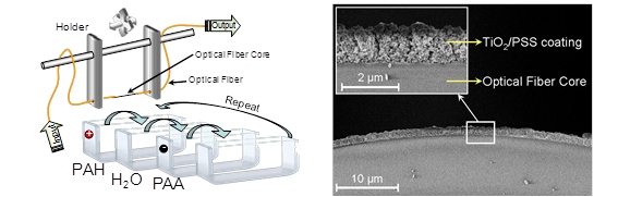
Fig1. Left: Schematic representation of the LbL fabrication process. Right: SEM image of [TiO2/Pss]70 coating fabricated onto the optical fiber core by using the LbL fabrication process
A number of parameters should be precisely controlled in order to achieve repeatable films, such as pH, concentration, ionic strength, curing temperature, or ratio between the poly-electrolytes used. The study and understanding of the fabrication of LbL structures onto optical fibers has been widely addressed by our group in the fabrication of diverse sensitive and functional coatings such as PAH/PAA, PDDA/PSS, PAH+NR/PAA, HPTS+PAH/PAA, SiO2+/SiO2-, TiO2/PSS, PAH+Ag/PAA, etc.
Electrospinning (ES)
Electrospinning processes are commonly used in industrial applications of the production of synthetic fibers from polymer solutions. In the electrospinning process, a polymeric solution is held at the end of a conductive capillary tube, which is subjected to an electric field that induces charge on the liquid surface. As the solution travels in air, due to the electric forces, the solvent evaporates, leaving behind a charged polymer fiber which lays itself randomly on a collecting metal screen or onto a different substrate, such as an optical fiber, placed in between as it is represented in Figure 2a. Depending on the fabrication parameters, electrospun fibers may have small diameter, ranging downward from 5 to 0.005 microns as it is represented in Figure 2b.
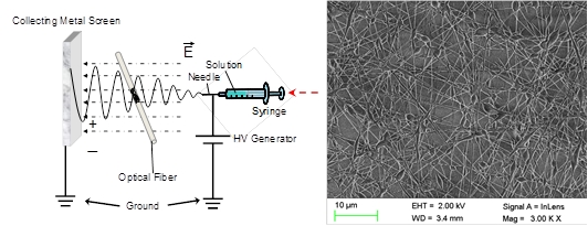
Fig2. Left: Schematic representation of the Electrospinning fabrication process. Right: SEM image of polymeric fibers fabricated onto the optical fiber core by using the electrospinning fabrication process.
Physical Vapour Deposition (PVD)
PVD technique is intended to be used onto planar substrates such as semiconductor wafers and does not enable the deposition of the films all around the fiber directly. In spite of that, slight modifications of the technique have been developed by our group to overcome that issue. An example consist of the utilization of rotation mechanisms placed into the deposition chamber (see Figure 3) that enables to produce thin-homogeneous coatings onto the optical fiber at nm scale precision using a wide range of materials such as Au, Ag, Mg, Cr, Pt, W, Indium tin oxide (ITO), etc.
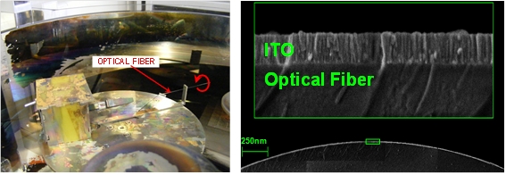
Fig3. Left: Mechanism employed to rotate the fiber inside the sputtering deposition chamber. Right: SEM image of the ITO coating fabricated using the sputtering technique.
Sol-Gel Dip-Coating Technique
Sol–gel dip-coating technology is one of the fastest growing fields of contemporary chemistry owing to its simplicity and versatility suitable to be used with optical fibers. The most important drawback of this technique is the lack of a precise film thickness control at the nanometric level ranging from 100 nm to 200 nm in average, which can be in part overcome by the precise control of the fabrication parameters such as the type of precursor, the pH, the nature and concentration of the catalyst, H2O:Si molar ratio, the type of co-solvent, temperature, method and extension of drying, the presence of doping substances or the pulling up speed. Apart from the disadvantage mentioned above, sol-gel technique provides a powerful, simple, flexible and low-cost processing technique that has led to the development of an ample variety of optical fiber sensing devices thanks in part to the easy way of doping.
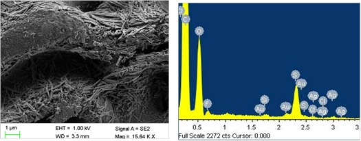
Fig4. Left: SEM image of a sol-gel vapochromic coating fabricated onto the optical fiber. Right: Composition of the coating fabricated onto the fiber.
Electrochemical deposition
Electrochemical deposition technique is commonly used in the manufacturing of products for our everyday lives. This technique has evolved from an art to a science and accordingly there have been many discoveries that pushed its use towards the deposition of nanoscale films. The special case of optical fiber constraints its utilization to a prior deposition of a metallic conducting film, by means of some of the previously described techniques. This enables the electrodeposition of a wider range of materials onto the optical fibers and the fabrication novel optical fiber chemical sensors and biosensors. However, the characteristics of the metallic coatings, such as the high absorption in the visible range, restrict the utilization of absorption or fluorescence measurements in most cases, which has been overcome by the breakthrough of transparent conducting oxides (TCOs) such as indium oxide or ITO (see Figure 5).
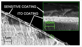
Fig5. SEM image of a NR/PAA pH-sensitive coating fabricated onto an ITO coated optical fiber using the electrodeposition technique.
Contact: Ignacio Matías, Francisco Javier Arregui, Cándido Bariain, Ignacio Del Villar, Javier Goicoechea, Carlos Ruiz, Cesar Elosua
Dpto de Ingeniería Eléctrica y Electrónica
Campus Arrosadia
Pamplona
Tel. +34 948 169055
Fax. + 34 948 169720
Contact by E-mail